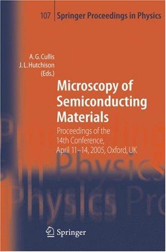
Microscopy of Semiconducting Materials
0
0
As an Amazon Associate and affiliate partner, Menrva Books earns from qualifying purchases. Learn more
Author Description
Author description coming soon. We're reaching out to them in the ether...
Menrva's Summary
THE THESIS
This book investigates the application of microscopy techniques to the study of semiconducting materials. It draws upon the expertise of A. G. Cullis, a recognized figure in the field, to present a comprehensive overview of advanced imaging methods. The work details the principles and practical applications of various microscopy techniques, focusing on their ability to reveal the intricate structures and properties of semiconductors at the nanoscale. It serves as a critical resource for researchers and students seeking to understand the material science behind modern electronic devices.
THE SCOPE MAP
- Detailed examination of Transmission Electron Microscopy (TEM) for semiconductor analysis.
- Coverage of Scanning Electron Microscopy (SEM) and its role in surface characterization.
- Exploration of Atomic Force Microscopy (AFM) for nanoscale imaging and property mapping.
- Discussion of specialized techniques such as High-Resolution TEM (HRTEM) and Scanning Tunneling Microscopy (STM).
- Analysis of defects, interfaces, and nanostructures in various semiconductor systems.
- Applications in device fabrication, material characterization, and fundamental research.
- Insights into sample preparation techniques crucial for high-quality microscopy.
- Case studies illustrating the power of microscopy in solving complex materials problems.
THE AUTHORITY PERSPECTIVE
This text is recognized as a significant contribution to the field of materials science, particularly for its in-depth exploration of microscopy techniques applied to semiconductors. It is regarded as a valuable reference for researchers and advanced students due to its technical rigor and comprehensive scope. The book's detailed approach to imaging and analysis provides essential insights for understanding semiconductor properties and developing new materials and devices.
Page Count:
600
Publication Date:
2006-01-01
ISBN-10:
354031914X
ISBN-13:
9783540319146
Art
Non-Fiction
Science
Physics
Engineering
Community Tags
Similar Books