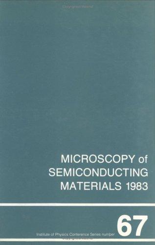
Microscopy of Semiconducting Materials, 1983
0
0
As an Amazon Associate and affiliate partner, Menrva Books earns from qualifying purchases. Learn more
Author Description
Author description coming soon. We're reaching out to them in the ether...
Menrva's Summary
THE THESIS
The book investigates the application of microscopy techniques to the study of semiconducting materials. It details the principles and practical implementations of various microscopy methods, including transmission electron microscopy (TEM) and scanning electron microscopy (SEM), as applied to semiconductor research. The text focuses on how these techniques reveal crystallographic defects, interfaces, and microstructural features crucial for understanding material properties and device performance. It serves as a technical reference for researchers and students in solid-state physics and materials science.
THE SCOPE MAP
- Detailed explanation of Transmission Electron Microscopy (TEM) for semiconductor analysis.
- Coverage of Scanning Electron Microscopy (SEM) and its applications.
- Analysis of crystallographic defects and their impact on material properties.
- Examination of interfaces and microstructural features in semiconductors.
- Discussion of imaging techniques for semiconductor device structures.
- Case studies illustrating the use of microscopy in materials characterization.
- Focus on the relationship between microstructure and electronic properties.
THE AUTHORITY PERSPECTIVE
This book is recognized as a specialized technical reference within the field of materials science and solid-state physics. Its detailed examination of microscopy techniques for semiconductors positions it as a valuable resource for researchers and advanced students. The content likely appeals to those requiring in-depth knowledge of microstructural analysis for semiconductor materials. The authority perspective suggests a text that is both informative and practical for laboratory applications.
Page Count:
520
Publication Date:
1983-01-01
ISBN-10:
0854981586
Non-Fiction
Science
Physics
Community Tags
Similar Books